

Business Sector
HOME > Business Sector > Printed Electronics (PE)
Printed Electronics Introduction
InkTec creates a new history in printed electronics
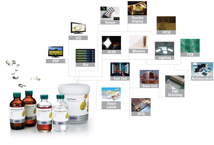
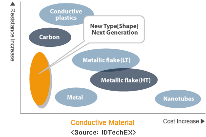
Printed Electronics substitutes the existing processes (etching/PL, metalizing, plating, etc. depending on the product) with the production of electronic devices or components using various functional materials in printing methods. We provide the great benefits of process improvements, pricing competitiveness, large-area/large-quantity production, and ecofriendly process application. Various functional materials can be used in printed electronics, such as metals (Ag, Cu, Al, etc.), CNT, BIO, Ceramic, Conductive Polymer, and molecules. The process may require additional materials like primers and insulators based on the applicable products.
Using printing processes, printed electronics brings the advantages of non-contact and dry processes. This can lead to the creation of products in new forms, using these processes or as replacements of existing products. They can be based on a variety of functional materials. These processes require high-resolution precision control, equipment technology, and complex process implementation technology.
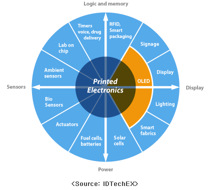
Printed Electronics can be applied in various industries such as Touch Screen Panels, Display, PCB, EMI Shielding, Printed Memory, Solar Cell, Lighting, Sensor, RFID, Signage, and Bio. We expect substantial advancement through the development of new functional materials and traditional printing techniques.
InkTec has been self-developing various materials that suit different printing methods to lead the printed electronics industry, and are supplying economical and productive materials and components through different printing techniques and optimized materials that we possess. Furthermore, we will further develop our business into an enterprise specializing in printed electronics through continuous development of functional materials.
Major Advantages of Printed Electronics
- Reduced loss of material cost, inexpensive manufacturing process and equipment cost
- Capable of large-area/large-quantity production and small productions of multiple products
- Applicability on diverse design changes
- Applicable for various flexible substrates (e.g. plastic films, foils and papers)
- Reduced emission of toxic substances & an environmentally-friendly process
Materials & Applicable Markets for Printed Electronics
- Areas where metallic ink (Au, Ag, Cu, etc.) is used
- Areas where ceramic ink is used
- Areas where molecular ink is used
Manufactured Goods by Printing Method
| Printing method | Applicable market | Applicable Substrate | Printing Form |
| Inkjet | TSP, PV, Sensor, Signage, Smart Label, Printed FPCB, Printed memory, etc (Common electrodes & patterning, etc.) |
Plastic Film, Glass, Paper |
Sheet to Sheet Roll to Roll |
| Screen Printing | |||
| Pad | |||
| Imprinting | |||
| Gravure Off-set | |||
| Flexography | Continuous printing-capable substrates | Roll to Roll | |
| Reverse Off-set | |||
| Gravure | |||
| Slot-die | |||
| Knife coating | |||
| Coating(Spin/Spray) | Decoration, Functional coating, surface treatment, etc. | Plastic Film, PC, ABS, etc |